Many fine-featured processes utilize CMP (Chemical-Mechanical Polishing) to
achieve planarity. Currently, all the 0.35 micron (and smaller) processes are
in this category. Effective CMP requires that the variations in feature density
on a layer be restricted. The following fill rules may be refined.
| xx.1 | Minimum poly layer density | 15% |
| xx.2 | Minimum metal layer density (applies separately to each metal layer other than the topmost one, which has no restriction) |
30% |
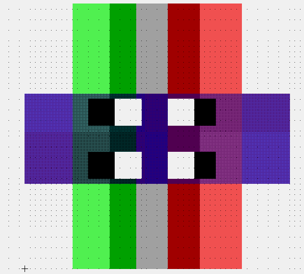
Many foundries quietly fills in the open areas on projects fabricated on the affected processes. The basic fill cell (see below) is 5 um x 5 um and consists of a properly connected stack of active, poly, and all the metals other than the topmost one. This cell is placed in any and all open areas of the projects. Open area, here, is any region that contains no {well or active or poly or any metal (including topmost)}, and is at least 5 um away from any such layout. Filling is thus confined to "large" open areas of the project (where large begins around 15 um square).
You may, therefore, choose to leave large, open regions, knowing that the foundry will fill them for you. Or you may choose to implement your own filling, so that you have complete control of your layout. The one situation that must be avoided under these minimum density rules is large non-empty regions that are devoid of one (or more) of the minimum density layers.
DS1 100/20;
(SCMOS 5 x 5 micron fill cell for levels up to metal3);
LCAA; B24 100 30 50;
LCPG; B28 100 68 50;
LCCC; B10 10 30 40;
      B10 10 30 60;
      B10 10 68 40;
      B10 10 68 60 ;
LCMF; B100 34 50 50;
LCVA; B10 10 40 40;
      B10 10 40 60;
      B10 10 60 40;
      B10 10 60 60;
LCMS; B34 100 50 50;
LCVS; B10 10 40 40;
      B10 10 40 60;
      B10 10 60 40;
      B10 10 60 60;
LCMT; B100 34 50 50;
DF;

C 1;
E
Process-Induced Damage (otherwise known as "Antenna Rules") Rules - General Requirements
The "Antenna Rules" deal with process induced gate oxide damage caused when exposed polysilicon and metal structures, connected to a thin oxide transistor, collect charge from the processing environment (e.g., reactive ion etch) and develop potentials sufficiently large to cause Fowler Nordheim current to flow through the thin oxide. Given the known process charge fluence, a figure of exposed conductor area to transistor gate area ratio is determined which guarantees Time Dependent Dielectric Breakdown (TDDB) reliability requirements for the fabricator. Failure to consider antenna rules in a design may lead to either reduced performance in transistors exposed to process induced damage, or may lead to total failure if the antenna rules are seriously violated.
The polysilicon rules require that the area of the polysilicon over field oxide divided by the area of the transistor gate (thin oxide area) must be less than Np (where Np is a limit that depends on the process and on design targets). For example, a 200um long by 1um wide polysilicon wire connected to two channel regions of 2um X 0.6um and 1um X 0.6um has an antenna ratio of 111. Usually the polysilicon rules are fairly conservative, so the antenna ratio in this example may be in violation of some fabricator's polysilicon antenna rule.
A similar calculation applies to metal wires connected to transistor gates. In this case, you must first obey the Np:1 rule for any polysilicon. Metal antenna rules can be a little more variable depending upon how conservative a fabricator is in dealing with this damage mechanism. The most conservative approach recognizes that process induced damage is a cumulative effect. In this case, you calculate the total area of the poly + metal 1 + metal 2 + metal 3 + ... and divide by the area of the transistor channels connected to this structure. This ratio must be less than Nm.
A less conservative metal antenna rule defines ratios for each metal level (Nm1, Nm2, Nm3, etc.) and recognize that lower levels of metal are protected by inter-level dielectric during the etch process for the metal above. Other metal rules recognize that photoresist covers metal lines during reactive ion etch, so the antenna rule only needs to consider the area of the exposed metal edges. This results in rules defined for area ratio calculations as follows: Ratio = 2[(L_metal+W_metal)*t_metal]/(W_channel*L_channel), where, W_metal, L_metal, and t_metal are the width, length and thickness of the metal line connected to a total channel area defined by W_channel by L_channel.
If metal 1 is connected to an active area junction and to a poly structure connected to a transistor channel, then the Nm:1 rule is relaxed. However, the poly Np:1 ratio rule STILL applies. The reason for this exception is that charge induced current is safely shunted through the junction to the substrate and, therefore, does not cause gate oxide damage. The junction area ratio (A_total/A_junction) must not be more than N_max:1. Note: A_total is the sum of poly and metal area connected to a thin oxide region.
An additional absolute area rule is also imposed for additional safety margin. The total area of exposed conductor that is electrically connected to a gate channel area limited to A_max um^2. Other constraints may apply, but these constraints are specific to a particular fabricator.
There are layout techniques to help deal with antenna ratio rules. For example, if a design uses a large array of clocked devices connected to a single clock source via a metal 1 clock distribution structure then a "cut and link" method can be used to moderate the antenna rule effects. In this method, the metal 1 distribution structure is divided up into pieces of metal 1 connected to gate structures such that the antenna rule is obeyed. Short links from metal 1 to metal 2 then back to metal 1 connect the clock distribution structure in a way that it prevents the total area of the clock distribution structure from being connected to gate poly structures during metal 1 etch. If the metal 2 links are the minimum links necessary to make the connection, then the current induced in the metal 2 area is very small (Nm2 << metal 2 rule).