Department of Electrical &
Electronic Engineering
MSc in Analogue and Digital IC Design (2018-2019)
Lab Experiment
Mastering Digital Design in Verilog using FPGAs
Department of Electrical &
Electronic Engineering MSc in Analogue and Digital IC Design (2018-2019) Mastering Digital Design in Verilog using FPGAs |
|
Aims
1. To ensure all students on the MSc course reaches a common competence level in RTL design using FPGAs in a hardware description language;
2. To act as revision exercise for those who are already competent in Verilog and FPGA.
You will conduct this experiment in the first half of the Autumn Term between 9th October and 10th November 2017. You can find a copy of the Experiment Specification Document here.
Team Pairing
You will be working in pairs for this experiment. I have group you together with random pairing. You can find which Lab Group you belongs and who is your Lab partner for this experiment here.
Learning Outcome
This Lab Experiment has FOUR distinct parts, each with specific learning outcomes.
Part 1: Basic competence in using Intel/Altera’s Quartus design systems for Cyclone-V FPGA; appreciate the superiority of hardware description language over schematic capture for digital design; use of case statement to specify combinatorial circuit; use higher level constructs in Verilog to specify complex combinatorial circuits; develop competence in taking a design from description to hardware.
Part 2: Use Verilog to specify sequential circuits; design of basic building blocks including: counters, linear-feedback shift-registers to generate pseudo-random numbers, basic state machines; using enable signals to implement globally synchronisation.
Part 3: Understand how digital components communicate through synchronous serial interface; interfacing digital circuits to analogue components such as ADC and DAC; use of block memory in FPGAs; number system and arithmetic operations such as adders and multipliers; digital signal generation.
Part 4: Understand how to implement a FIFO using counters as pointer registers and Block RAM as storage; implement a relatively complex digital circuit using different building blocks including: counters, finite state machines, registers, encoder/decoder, address computation unit, memory blocks, digital delay elements, synchronisers etc.; learn how to debug moderately complex digital circuits.
Assessment
There will be an oral interview at the end of the xxperiment. The marks for this experiment will count towards the MSc course Coursework Component.
The Experiment Handbook (all four parts) can be found HERE.
Experiment |
Useful Resources |
|
|
|
|
|
|
Lectures
Lecture 1 - Introduction (12 Oct) - Notes(X1), Notes(X2)
Lecture 2 - Clock circuits (19 Oct) - Notes(X1), Notes(X2)
Lecture 3 - PWM, FSM & SPI (26 Oct) - Notes(X1), Notes(X2)
Lecture 4 - Echo Synthesizeer (2 Nov) - Notes(X1), Notes(X2)
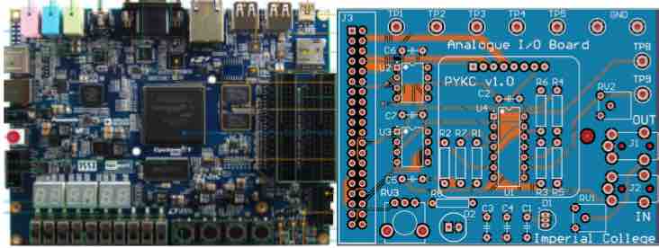
DE1-SoC Reference Manuals
DE1-SoC Board from Terasic
DE1-SoC Learning Roadmap
DE1-SoC Getting Started Guide
DE1-SoC My First FPGA
DE1-SoC User's Manual
DE1-SoC Schematic Diagram
Cyclone V Device Handbooks
Cyclone V Device Overview
Cyclone V Device Handbook Vol 1: Device Interfaces and Integration
Cyclone V Device Handbook Vol 2: Transceivers
Cyclone V Device Handbook Vol 3: Hard Processor System Technical Reference Manual
Quartus Related Links
Quartus Prime Lite Web Edition (free)
Quartus Tutorial Page (containing MANY tutorials, probably too many. Be selective!)
Verilog Resources
Verilog tutorial by ASIC World