Vision
|
Current
Research
|
Achievements
|
Publications
|
Vision
Semiconductor technology is aiming at higher speeds and smaller dimensions for everyday applications. Si technology will soon reach the limit where quantum effects will severely disrupt the functioning of the "classical" devices. Therefore we aim to use different materials which improve the characteristics without reaching the quantum limit or we use the quantum effect itself to make highly functional devices. Progress in the Si microelectronics field does not necessarily lie only in aggressive downscaling and development of gate stacks. One also has to look into alternative geometries that can offer higher functionality or improved robustness against downscaling. In the move towards nanotechnology one realises that the strictly organised fabrication techniques that are currently used, are not always the most appropriate or the most cost-effective. Self-assembly of nanostructures and the development of efficient techniques to make circuits and systems with these self-assembled nanostructures are the current challenges. Critical thought has to be given to how and where these nanosystems will prove their potential for which they are advertised. Their potential may not lie in the traditional CMOS industry but in niche markets, existing and new, such as for instance thermoelectricity.
Current Research
 My
interests lie in the physics and applications of semiconductor devices based on
new material systems or quantum mechanical effects in IV-IV and III-V
materials, with the purpose of optimising existing device/circuit applications
in speed and functionality.
My
interests lie in the physics and applications of semiconductor devices based on
new material systems or quantum mechanical effects in IV-IV and III-V
materials, with the purpose of optimising existing device/circuit applications
in speed and functionality.
Over the last 10 years my research has concentrated on strained-Si technology on globally strained substrates. Different aspects of strained-Si technology were studied: the origin of the performance enhancement, the device performance for low power, the low frequency noise as a function of Ge concentration, Ge implantation and condensation for SGOI and two novel material characterisation techniques BKFM and CABOOM. More info on these topics can be found in the link to my research summary below. We received the best paper award on behalf of microelectronics reliability at the MIEL’08 conference for our work on the use of low frequency noise measurements to investigate the impact of processing on spintronics devices (see picture left).
Recently I have invented the screen-grid FET – a novel field effect transistor structure
with a particular gating configuration. TCAD modelling gives promising results
for both analogue as well as digital operation under aggressive downscaling.
Much of the pros and cons of this device have been recently presented at the
WOFE 2007 workshop. This link to the poster
presented at WOFE 2007 will give an idea of the analogue performance of the
device. Our team has received one of the best invited
papers awards for their work on the analogue and digital performance of
the SGrFET in WOFE’07. SGrFETs have
been made by Mir Enterprises,
 Another
exciting research topic that is being explored at the moment is that of Si
nanowire arrays for thermo electricity.
It has been shown by groups in e.g. MIT (M.S.
Dresselhaus), JPL (J.P. Fleurial) and the
Another
exciting research topic that is being explored at the moment is that of Si
nanowire arrays for thermo electricity.
It has been shown by groups in e.g. MIT (M.S.
Dresselhaus), JPL (J.P. Fleurial) and the
The team consisting of Paul Mitcheson, Roberto di Napoli and Kristel Fobelets are developing a virtual interactive web – EE-VIL – that will link the wide multidisciplinary area consisting of physics – microelectronics – circuit design. The purpose is for students to investigate cause and effect. For instance one can investigate that making changes in certain material parameters will cause the circuit, based on this material, to behave in a different way
For more research results, see this page.
Achievements
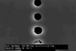
v Development of processing methods on InAs/AlSb/GaSb for resonant tunnelling components and small bandgap field effect transistors.
v Development of GaAs/AlAs micromachining methods have resulted in the construction of 1 micrometer thick membranes. Within these membranes a resonant tunnelling diode resides that acts as a pressure sensor. This demonstrated the first resonant tunnelling diode pressure sensor.
v Development of SiGe material characterisation techniques including CABOOM and bevel-KFM. These processes rely on the sensitivity of the oxidation processes on the Ge contents in the layer and on bevelling techniques. In CABOOM the thickness of the oxide is evaluated using light interference and maximum likelihood data processing to extract the Ge contents. In bevel-KFM an AFM is used to probe the workfunction differences between the AFM probe tip and the SiGe surface. Data analysis gives the Ge concentration.
v Low temperature investigations on strained-Si devices have brought the physical factors that influence the device performance to the foreground.
v Invention of screen-grid field effect transistor (SGrFET) for analogue and digital applications and for bio-sensing systems. The multi-gate character of the SGrFET gives excellent opportunities for digital circuits with a minimum number of components. This research has received at of the best invited paper awards on the WOFE’07 conference.
v The use of low frequency noise measurements as a tool to investigate the influence of processing on the device characteristics. This technique has given an insight into diffusion related problems in spintronics devices. We received the best paper award on behalf of microelectronics reliability at the MIEL’08 conference for this work. We are currently presenting an overview into the aspects of low frequency noise in n-channel strained-Si FETs.
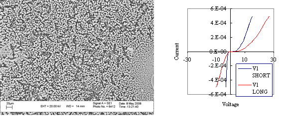
v The use of polymer based modulation doping techniques to control the conductivity in high resistivity p and n-type Si nanowires.