Microelectronics and Nanotechnology
Contents
Sub-micron Buried channel Heterojunction
Field Effect Transistors
Sub-micron Buried channel Heterojunction
Field Effect Transistors for low power circuits
SiGe-on-insulator
(SGOI) by Ge+ ion implantation
Si:SiGe MOSFET-on-air through post-processing
techniques
Low temperature operation of strained-Si and
SiGe MOSFETs and HFETs
Low Temperature and noise characteristics
modeling in strained-channel FETs
CABOOM: Characterisation of Alloy
concentration by Bevelling, Oxidation and Optical Microscopy
BKFM : Kelvin Probe Microscopy on bevelled samples
as material characterisation technique
The current Team
|
Dr. K. Fobelets
(Senior Lecturer) |
|
Prof. J.E. Velazquez-Perez (visiting professor) |
|
Ms. P.W. Ding (PhD) |
|
Ms. Y. Shadrokh
(PhD) |
The 2007-2008 undergraduate Team
|
Mr. Eng Kwee Guan
(Modelling of the SGrFET for biomolecule detection) |
|
Mr. Annamalai
Subramanian (TCAD of Si nano island chain transport) |
|
Ms. Evona T. T.
Teh (Control of dispersion of Au colloidal solution on Si) |
|
Mr. Jason
Chan (Chemical safety management) |
Final year research project students and MSc project
students of Imperial College London often contribute to the research of the
team. Their contributions are gratefully acknowledged.
Sub-micron Buried channel Heterojunction Field Effect Transistors
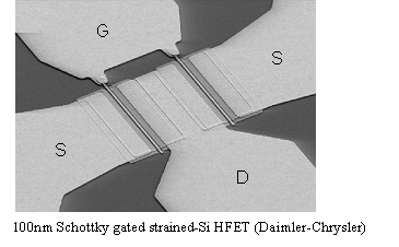
This EPSRC supported project in collaboration with Thomas Hackbarth
and Ulf Konig from
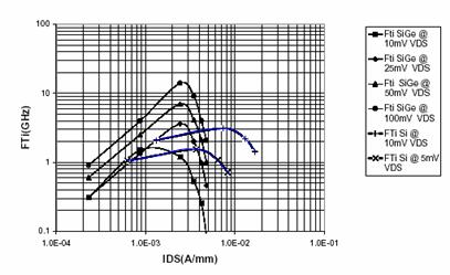
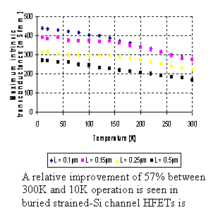
Intrinsic cut-off frequency vs. current density of the 100nm gate length HFET (100mm
gate width) and Si MOSFET (blue lines) (40mm gate width) for
different VDS values.
Sub-micron Buried channel Heterojunction Field Effect Transistors for low power circuits
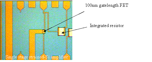
Kristel
Fobelets, et al.
This EPSRC supported project in collaboration with Thomas
Hackbarth and Ulf Konig from Daimler-Chrysler, Germany, aims to demonstrate the
low power RF capabilities of Schottky-gated strained-Si buried channel Field
Effect Transistors (HFET) monolithically integrated circuits. The circuits are
processed in Daimler-Chrysler. The design of masks and the DC/RF
characterisation of the circuits are done by the teams of K. Fobelets and C.
Papavasilliou. We have, as one of the first in the world, demonstrated RF
operation at low input power of some simple monolithically integrated HFET
circuits [papers].
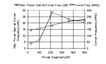
Single stage amplifier driven below threshold (VDS<0.3V,
VGS<-0.2V).
results: 15 dB gain @ 26 µW input power,
bandwidth 38 MHz .
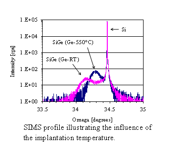
SiGe-on-insulator (SGOI) by Ge+
ion implantation
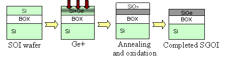
Kristel Fobelets, Hyung-Sang Yuk et al.
SOI
(Silicon-on-Insulator) has been accepted in mainstream CMOS technology and strained-Si
is being considered as a Si alternative MOS material, the need for
strained-SiGe-on-insulator (SGOI) is appearing. Different fabrication ways
exist, based on adapted SIMOX and Bonded-etch-back techniques. We have taken
the route of Ge+ implantations (collaboration with T. Tate) into commercial
SOI. Controlling implantation and anneal ambient we are working towards a 30%
fully relaxed SGOI. Characterisation techniques employed, include XRD, SIMS,
TEM and Raman spectroscopy that are done externally in collaboration with HMOS
(EPSRC) project partners
[papers].
Si:SiGe MOSFET-on-air through post-processing techniques
K. Fobelets, S.M. Li et al.
Completely processed MOS-gated Si/SiGe n-channel Modulation Doped Field
Effect Transistors (MODFETs) have been post-processed to remove the Si
substrate and part of the SiGe virtual substrate to construct strained-Si
MOSFETs-on-air. The resulting substrate thickness underneath the devices was
reduced down to 2 mm after thinning and a flip-chip process was developed to
transfer the devices to an insulating carrier substrate. A post-processing
technology was developed for heat sensitive devices. The membrane devices,
surrounded by air, were characterised after thinning and compared to the
un-thinned characteristics. A large reduction of the off-currents of the
MODFETs on air, due to an increase in substrate resistance, has been measured,
making them more suitable for low power applications. Further relaxation of the
substrate during substrate thinning causes a shift in the threshold voltage [papers].
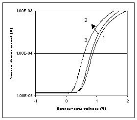
Top:
thinned devices front and back.
Bottom: 1,2,3 refer to further thinned substrates. We notice: a reduction of off-current due to decreased substrate leakage and shift in threshold voltage due to increased relaxation of virtual substrate
Low temperature operation of strained-Si and SiGe MOSFETs and HFETs

Kristel Fobelets,
Valerio Gaspari et al.
Low temperature
operation of strained-channel nMOS and pMOS is being studied using a closed
cycle cryostat operating between 10 and 350K with a precision of 1K. Comparing
low T operation of Si MOSFETs to strained-Si (SiGe) MOSFETs we generally see a
larger improvement in typical DC characteristics such as transconductance in
the strained-channel devices. Decreasing the operation temperature not only
removes certain scattering processes but also improves confinement of carriers.
Low temperature characterization of devices is a useful technique to study the
physical processes and leads potentially towards space applications where both
low temperature and low power are issues [papers].
Low Temperature and noise characteristics modelling in strained-channel FETs
Jesus-Enrique Velazquez-Perez (Univ.
A 2-D device
simulator – MEDICI - is used to study different effects occurring in
strained-Si channel MOSFETs. We have used MEDICI to study and solve the
backgating effect in these structures. Combination of MEDICI with
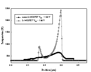
Electron temperature’s profile in the channel of a strained-Si MOSFET and a
conventional MOSFET calculated with MEDICI.
CABOOM: Characterisation of Alloy concentration by Bevelling, Oxidation and Optical Microscopy
Kristel Fobelets, Ryan Ferguson, et al.
The group has invented a novel, fast and inexpensive technique
to characterise the Ge concentration in heterojunctions using: a) shallow angle
bevelling to present the different layers in the heterojunction at the surface,
b) wet thermal oxidation will cover each layer of the heterojunction with an
oxide. As the oxidation rate of SiGe is dependent on the Ge concentration the
oxide thickness on the surface will be directly related to the Ge concentration
in the layer underneath. c) Optical microscopy to visualise the different oxide
thicknesses via diffraction. A program has been written in MathematicaTM
to calculate the Ge concentration from the coloured perceived under the
microscope. This program takes into account the spectrum of the microscope lamp
and the sensitivity of the eye and the RGB representation on the computer
screen [papers].
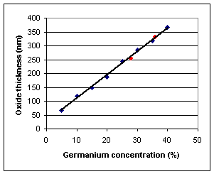
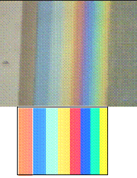
Left
top: A heterojunction with 8 layers with different Ge concentration bevelled
and oxidised, as seen under the optical microscope. The steps in Ge contents
are only 5% going from 0% (left) to 40% (right). Left bottom: the output of the
mathematica program gives the closest colour match and the associated Ge
concentration. Right: squares are the derived oxide thickness as a function of
Ge concentration for wet thermal oxidation at
700ºC for 1hr and the red circle are values found in literature for the same
oxidation conditions.
BKFM : Kelvin Probe Microscopy on bevelled samples as material characterisation technique
Kristel
Fobelets, Ryan Ferguson et al.
Bevelling is used in some material
characterisation techniques to enlarge the width of the thin layers in
heterojunctions. We have proposed a new technique to determine the thickness of
the layers and the material composition based on bevelling in conjunction with
Kelvin Probe Microscopy. A chemical-mechanical polishing technique has been
developed to generate nanometer smooth bevels, important to generate
un-convoluted signals. Germanium quantum wells of only 7.5 nm wide have been
successfully imaged using KFM, while material composition differences of only
5% can be visualised under an optical microscope. Work function differences
between the different layers can be measured, and material compositions can be
theoretically determined to an accuracy of 1%. This simple and in-expensive,
high resolution technique might become a powerful tool in fast in-expensive
material characterisation technology [papers].
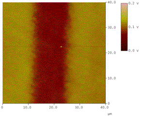
Top: A KFM image of a 20nm InAs
quantum well surrounded by GaSb cladding layers after bevelling
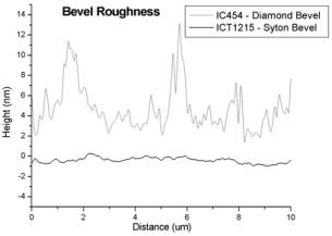
Bottom: Comparison between the
"classical" diamond bevel and the newly developed CMP bevel
roughness.
The Screen-Grid FET
SiO2
![]()
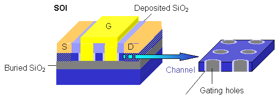
A novel 3D Field Effect Transistor on
SOI – screen-grid FET (SGFET) – is presented. The most important novel feature
of the SGFET is the design of the 3D gate cylinders which are embedded in the
channel and which allow great flexibility in device and gating geometry to
optimize performance. The floating body effect is avoided and the double gating
row configuration diminishes short channel effects. The traditional intimate
relationship between gate length and source-drain distance is lost, resulting
in and easy control of drain induced barrier lowering, improved output
conductance and ideal sub-threshold slope. The separation between the gate
fingers in each row is the key factor to optimize the performance whilst
downscaling of the source-drain distance is not essential from an operational
point of view. Due to the extra geometrical parameters in the SGFET, short
channel effects can be controlled without causing associated detrimental
effects [papers].
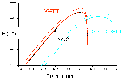
Cut-off frequency as a function of
current level for the SGFET compared to an SOI MOSFET of the same geometry.